تاريخ الفيزياء
علماء الفيزياء


الفيزياء الكلاسيكية
الميكانيك
الديناميكا الحرارية
الكهربائية والمغناطيسية
الكهربائية
المغناطيسية
الكهرومغناطيسية
علم البصريات
تاريخ علم البصريات
الضوء
مواضيع عامة في علم البصريات
الصوت
الفيزياء الحديثة
النظرية النسبية
النظرية النسبية الخاصة
النظرية النسبية العامة
مواضيع عامة في النظرية النسبية
ميكانيكا الكم
الفيزياء الذرية
الفيزياء الجزيئية
الفيزياء النووية
مواضيع عامة في الفيزياء النووية
النشاط الاشعاعي
فيزياء الحالة الصلبة
الموصلات
أشباه الموصلات
العوازل
مواضيع عامة في الفيزياء الصلبة
فيزياء الجوامد
الليزر
أنواع الليزر
بعض تطبيقات الليزر
مواضيع عامة في الليزر
علم الفلك
تاريخ وعلماء علم الفلك
الثقوب السوداء
المجموعة الشمسية
الشمس
كوكب عطارد
كوكب الزهرة
كوكب الأرض
كوكب المريخ
كوكب المشتري
كوكب زحل
كوكب أورانوس
كوكب نبتون
كوكب بلوتو
القمر
كواكب ومواضيع اخرى
مواضيع عامة في علم الفلك
النجوم
البلازما
الألكترونيات
خواص المادة
الطاقة البديلة
الطاقة الشمسية
مواضيع عامة في الطاقة البديلة
المد والجزر
فيزياء الجسيمات
الفيزياء والعلوم الأخرى
الفيزياء الكيميائية
الفيزياء الرياضية
الفيزياء الحيوية
الفيزياء والفلسفة
الفيزياء العامة
مواضيع عامة في الفيزياء
تجارب فيزيائية
مصطلحات وتعاريف فيزيائية
وحدات القياس الفيزيائية
طرائف الفيزياء
مواضيع اخرى

JFET biasing
 المؤلف:
Stan Gibilisco
المؤلف:
Stan Gibilisco
 المصدر:
Teach Yourself Electricity and Electronics
المصدر:
Teach Yourself Electricity and Electronics
 الجزء والصفحة:
419
الجزء والصفحة:
419
 12-5-2021
 2834
2834


+
-
20
JFET biasing
Two biasing arrangements for an N-channel JFET are shown in Fig. 1. These hookups are similar to the way an NPN bipolar transistor is connected, except that the source-gate (SG) junction is not forward-biased.
At A, the gate is grounded through resistor R2. The source resistor, R1, limits the current through the JFET. The drain current, ID, flows through R3, producing a voltage across this resistor. The ac output signal passes through C2.
At B, the gate is connected to a voltage that is negative with respect to ground through potentiometer R2. Adjusting this potentiometer results in a variable negative EG between R2 and R3. Resistor R1 limits the current through the JFET. The drain current, ID, flows through R4, producing a voltage across it; the ac output signal passes through C2.
In both of these circuits, the drain is positive relative to ground. For a P-channel JFET, reverse the polarities in Fig. 1. The connections are somewhat similar to the way a PNP bipolar transistor is used, except the SG junction isn’t forward-biased.
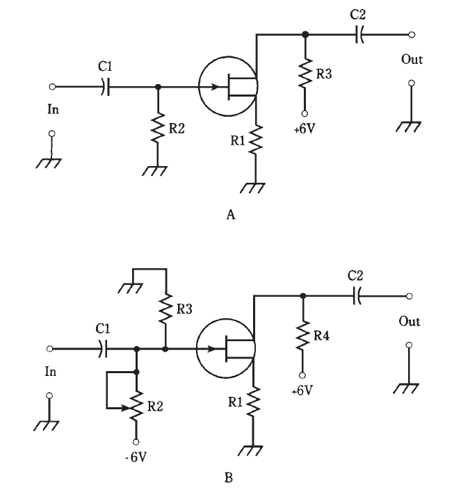
Fig. 1: Two methods of biasing an N-channel JFET. At A, fixed gate bias; at B, variable gate bias.
Typical JFET power-supply voltages are comparable to those with bipolar transistors. The voltage between the source and drain, abbreviated ED, can range from about 3 V to 150 V; most often it is 6 V to 12 V.
The biasing arrangement in Fig. 1A is commonly used for weak-signal amplifiers, low-level amplifiers and oscillators. The scheme at B is more often employed in power amplifiers having a substantial input signal.
 الاكثر قراءة في الألكترونيات
 اخر الاخبار
اخبار العتبة العباسية المقدسة

الآخبار الصحية


مواضيع ذات صلة
 قسم الشؤون الفكرية يصدر كتاباً يوثق تاريخ السدانة في العتبة العباسية المقدسة
 "المهمة".. إصدار قصصي يوثّق القصص الفائزة في مسابقة فتوى الدفاع المقدسة للقصة القصيرة
 (نوافذ).. إصدار أدبي يوثق القصص الفائزة في مسابقة الإمام العسكري (عليه السلام)