تاريخ الفيزياء

علماء الفيزياء


الفيزياء الكلاسيكية

الميكانيك

الديناميكا الحرارية


الكهربائية والمغناطيسية

الكهربائية

المغناطيسية

الكهرومغناطيسية


علم البصريات

تاريخ علم البصريات

الضوء

مواضيع عامة في علم البصريات

الصوت


الفيزياء الحديثة


النظرية النسبية

النظرية النسبية الخاصة

النظرية النسبية العامة

مواضيع عامة في النظرية النسبية

ميكانيكا الكم

الفيزياء الذرية

الفيزياء الجزيئية


الفيزياء النووية

مواضيع عامة في الفيزياء النووية

النشاط الاشعاعي


فيزياء الحالة الصلبة

الموصلات

أشباه الموصلات

العوازل

مواضيع عامة في الفيزياء الصلبة

فيزياء الجوامد


الليزر

أنواع الليزر

بعض تطبيقات الليزر

مواضيع عامة في الليزر


علم الفلك

تاريخ وعلماء علم الفلك

الثقوب السوداء


المجموعة الشمسية

الشمس

كوكب عطارد

كوكب الزهرة

كوكب الأرض

كوكب المريخ

كوكب المشتري

كوكب زحل

كوكب أورانوس

كوكب نبتون

كوكب بلوتو

القمر

كواكب ومواضيع اخرى

مواضيع عامة في علم الفلك

النجوم

البلازما

الألكترونيات

خواص المادة


الطاقة البديلة

الطاقة الشمسية

مواضيع عامة في الطاقة البديلة

المد والجزر

فيزياء الجسيمات


الفيزياء والعلوم الأخرى

الفيزياء الكيميائية

الفيزياء الرياضية

الفيزياء الحيوية

الفيزياء والفلسفة

الفيزياء العامة


مواضيع عامة في الفيزياء

تجارب فيزيائية

مصطلحات وتعاريف فيزيائية

وحدات القياس الفيزيائية

طرائف الفيزياء

مواضيع اخرى
LASER STRUCTURE
المؤلف:
Mark Csele
المصدر:
FUNDAMENTALS OF LIGHT SOURCES AND LASERS
الجزء والصفحة:
p315
14-4-2016
5287
LASER STRUCTURE
The simplest (and oldest) structure for a laser diode is the homojunction laser diode, which uses a single junction. These are fabricated of a single junction between two direct-band gap materials of the same type, one p-type and one n-type, that is called a homojunction since both materials are of the same type. Light is emitted by electron hole pair recombinations in the thin active region formed by the junction of the two materials (the depletion region). Usually, gallium arsenide (GaAs) is used, with each part of the device doped slightly differently: one part with an electron donor and one part with an electron acceptor. Mirrors for the laser cavity are fabricated simply by cleaving the crystal at right angles to the laser axis. Having an index of refraction of 3.7, the reflectivity of each mirror may be calculated to be 33% by using the Fresnel equations. This represents a large loss in the cavity; however, most semiconductor laser materials have ample gain, to allow such a simple configuration. Improved performance may be achieved by fabricating a single dielectric mirror, composed of alternating quarter-wavelength-thick layers of high- and low-index-of-refraction materials, at the HR end of the laser diode. Improved mirrors are used on almost all modern laser diodes. A diagram of a simple homojunction structure is shown in Figure 13.2.1. Homojunction lasers are characterized by large threshold currents with a typical device requiring tens of amperes to lase. Such currents prohibit continuous operation at room temperature, so CW homojunction devices require cryogenic cooling, making them impractical for many applications.

Figure 1.1. Homojunction laser structure.
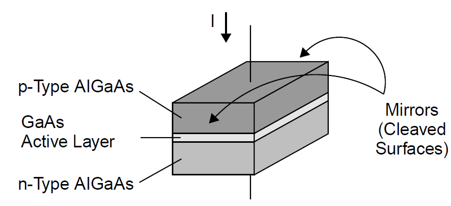
Improvements in the structure of the laser may be made by confining the intracavity beam in a dielectric waveguide structure formed from the semiconductor material itself. Such a structure requires two interfaces of different indexes of refraction, one on top and one below the active region, so two junctions are formed in what is called a heterostructure laser diode, or in this case, a double heterostructure, since there are two confining interfaces. To obtain different indexes of refraction, two different materials are required. GaAs is generally used as the higher-index material and aluminum gallium arsenide (AlGaAs) as the lower-index material. As depicted in Figure 1.2, AlGaAs is doped to form p- and n-type materials which essentially have identical indexes of refraction given that dopant concentration is small. Between layers of these materials, GaAs is sandwiched as the active-region material, from which laser light is emitted. Differences between the indexes of refraction occurring at each interface form a reflector that confines light inside the GaAs layer, which drastically improves efficiency, and more important, lowers threshold current for the device by increasing gain. The active region (GaAs) is typically only 0.1 μm in thickness.
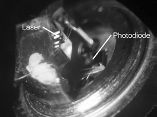
Usually, a stripe contact is used on the top of the structure to make an electrical connection to the device. This further limits the area of the active region in the GaAs laser (since current is not spread out over the top surface area of the entire structure), which serves to increase current density and further lower threshold current. In a real laser diode of this type, more than three layers are generally required, and a layer that serves as an electrical interface between metal contacts and each AlGaAs layer is usually employed. Double-hetero junction laser diodes commonly operate at room temperatures with low threshold currents, in the tens-of-milli amperes range. A commercially available diode laser of this type is shown in Figure 1.3, in which the diode itself is the small crystal (in reality, the size of a grain of salt) mounted atop a block of metal that serves as a heatsink. Behind the laser crystal is a photodiode that serves to supply the driver circuitry with feedback about the actual light level emitted from the laser, allowing the circuit to stabilize the laser output power.
The double-heterostructure arrangement confines intracavity light in only one direction (top and bottom) of the GaAs layer, but a further improvement in performance can be made by manufacturing the device so that a confining dielectric interface exists on all four sides of the active region in a buried heterostructure

Figure 1.2. Hetero junction laser structure.

Figure 1.3. Typical laser diode.
laser, depicted in Figure 1.4. In such an arrangement the entire stack of three layers of a typical hetero junction laser (p-type AlGaAs, GaAs active region, and n-type AlGaAs) is confined on each side by an n-type AlGaAs layer. The interface between the GaAs material in the active region, and this lower-index-of-refraction material on the sides of the active layer, serves to further confine light in the laser cavity. Such lasers are often called index guided, since light inside the cavity is guided in a manner similar to that of an index-graded fiber optic.
One of the newest structures for semiconductor lasers is the vertical cavity surface- emitting laser (the VCSEL). In a laser of this type, light is not emitted from the edge of the device but rather through the entire top layer of the semiconductor crystal itself. While edge-emitting laser diodes produce an elliptically shaped output beam that has high divergence, requiring an external lens to collimate it into a usable beam, a VCSEL produces a round beam of much higher quality. Rather than emission from the edge of the diode, light is emitted from the surface of a VCSEL. In addition to a better beam shape, VCSELs feature single longitudinal mode operation with a narrow spectral linewidth.
A VCSEL features a thin active layer (100 to 200 nm) like that of a conventional laser diode, but whereas the gain length of a conventional diode is 200 to 500 μm

Figure 1.4. Buried hetero junction laser structure.
(the length of the structure), the gain length in a VCSEL is the length of the active layer. Resonator optics are fabricated above and below the semiconductor crystal. With a short active layer and low gain, cavity optics must be fabricated from multiple layers of dielectrics alternating quarter-wavelength-thick layers of high- and low-index-of-refraction materials for high reflectivity. Current in the device flows along the optical axis through electrodes on the top and bottom of the device instead of perpendicular to it. These electrodes can be fabricated so that current flows through the mirror structure itself or through two contact layers close to the junction, the latter approach offering a lower electrical resistance. The typical structure of a VCSEL is depicted in Figure 1.5.
The output from the VCSEL is preferred for coupling to a fiber since emission occurs in the form of a circular beam which is easily focused, as opposed to the elliptical output beam from an edge emitter. Aside from applications in which the output is coupled to optical fibers for communications use, VCSELs are also used in some newer designs, in which a frequency-doubling crystal is placed inside the cavity (or at least an extended cavity with three reflectors) of the semiconductor laser. The structure of the device allows the inclusion of wavelength-selective Bragg reflectors for resonator optics.
VCSEL lasers usually feature low threshold currents, often below 1 mA. Since the device does not require precision-cleaved ends to form cavity mirrors nor the deposition of multiple dielectric layers on the edges of the crystal, they may be fabricated as multiple devices on a single wafer in a manner similar to the method in which microchips are manufactured. Given the quality of the output beam as well as the low threshold of the device this is likely the most important up-and-coming device for optical communications.
Finally, it is possible to optically-pump some solid-state materials. One design uses an 808-nm pump diode to optically pump a 946-nm semiconductor laser which is, in turn, frequency doubled to produce 488-nm light. The arrangement, called a VECSEL (for vertical external cavity surface-emitting laser), has external optics allowing inclusion of a nonlinear crystal inside the cavity to accomplish frequency doubling. This particular laser, which has more in common with a diode-

Figure 1.5. VCSEL laser structure.
pumped solid-state laser than a semiconductor laser, is designed as a replacement for the blue argon-ion laser.
 الاكثر قراءة في مواضيع عامة في الليزر
 اخر الاخبار
اخبار العتبة العباسية المقدسة

الآخبار الصحية


 قسم الشؤون الفكرية يصدر كتاباً يوثق تاريخ السدانة في العتبة العباسية المقدسة
 "المهمة".. إصدار قصصي يوثّق القصص الفائزة في مسابقة فتوى الدفاع المقدسة للقصة القصيرة
 (نوافذ).. إصدار أدبي يوثق القصص الفائزة في مسابقة الإمام العسكري (عليه السلام)


